Translate

Saturday, September 19, 2015

How to use the TFT display 2.2" QVGA with Arduino, Part 1/2

Arduino applications with ILI9341 library (Part 1/2)

By Giovanni Carrera 
Introduction
The main purpose of this project is to build a system based on chip ATMEGA328P, Arduino compatible, and interface it with a 2.2" QVGA TFT display using the library ILI9341. As an alternative to the self-build system you can use an Arduino Pro 3.3 V/ 8 MHz board or similar.
This system works well and can be very useful for many applications, as data-loggers, graphic terminal, etc. A great advantage of this system is to operate at 3.3 V with a modest power (180 mW). It is very suitable to be powered by a lithium 3.6V rechargeable battery. The regulator adopted still works well with a typical drop-out of about 50mV at low currents.
The display
After buying a TFT graphic display for few euros I decided to use it with Arduino. As often happens, the device was not at all documented by the seller neither by the manufacturer. However, the most salient features were screen-printed on the board. The graphics resolution was very good, QVGA means ¼ VGA, i.e. half of the pixels on each side, then 240x320 points to 64K or 256K colors. The interface used is the SPI. On the back of the card it is also a connector for SD card, very suitable to load images or save data. After searching on various forums and sellers in the internet, not without some difficulty, I were able to locate the object, finding a very synthetic scheme, a data sheet of the display and its controller  ILI9341 of Ilitek. By forum came out the link that allowed to download the library Seeed ILI9341 2.2 TFT + SD by Albert Miao, Loovee and Visweswara (https://github.com/gmtii/ili9341-arduino). The next photo shows the look of the TFT display used.
  
The first thing to do was to find out the power supply module, indicated by the abbreviation Vcc. I had to supply the module to 5 or 3.3V? Not even the scheme was to help. On it was indicated only the output voltage of the regulator: 3V, typical supply voltage of the display and the controller, as is apparent from the respective data sheet. On the card was a smd regulator whose name was different from that of the diagram and I did not find its data sheet in the internet. Surely it had to be a low-dropout regulator. I then, decided to supply the module with a voltage of 3.3V as a voltage drop of 0.3V is usually well tolerated by regulators with low drop-out, for currents of relatively modest also the use of 5V could have overheat, if not destroy, the tiny controller.
Hardware
Having already experienced the self-construction on the bread boards using the Arduino chip ATMEGA328P programmed with boot-loader, I decided for a version  powered to 3.3V instead of the classic 5 V. This is possible because the chip ATmega328P works also at lower voltages (1.8V), and has a less consumption. But the quartz in this case should be 8 MHz instead of 16, I have tried to overclock to 16 without having problems. The 3.3 V power supply simplifies interfacing of the display with the CPU, which otherwise require level converters. I programmed the chip with the Arduino bootloader, but it is easy to buy the chips already programmed. To load the sketch I used a USB serial converter module connected to a PC. The following figure shows the prototype and component layout.

To show the details of the card the display module was removed, it is connected to the board via a 9-pin strip connector (TFT interface) and a 4-wire cable and connector (SD interface). The display is fixed to the board by means of two nylon spacers. On the right it can be see the module that provides to convert the signals of the UART to USB. Below you can see the complete scheme of my system.
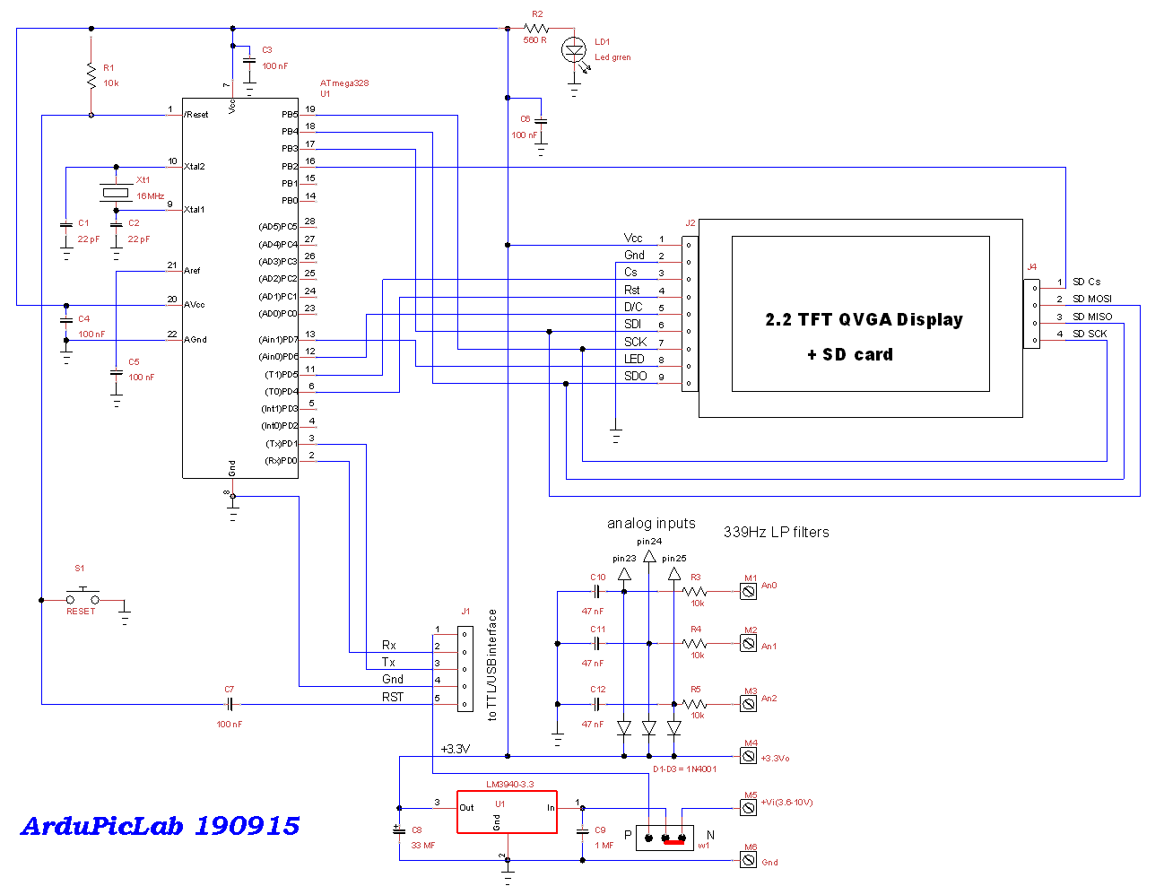
You can see the three filters RC low-pass anti-aliasing, with values ​​below the pulsation of cut is equal to:  w=1/(RC),  which corresponds to a frequency of about 340Hz. The three diodes act as protection for voltages greater than 3.3V. The low dropout regulator used is a LM3940-3.3, but you can replace it with an equivalent. The current consumption with display on and is about 50mA.
The image below shows the prototype in operation and with the sketch of test loads, which displays the measures of three analog channels.
When using the Arduino IDE to compile the sketch and send it to the system, it must indicate that the board used (Tools menu) is a "Arduino Pro" clocked by 16MHz and ATmega328 processor. This is a card without USB interface very similar to that proposed.
As showed in the scheme, the first three analog channels are wired to the terminal blocks because I want  to use the prototype to show these measurements on the display and store the data on an SD card.

Serial programming.
This little board is used only to program the card. The module serial / USB should work with the signals Tx, Rx and DTR as well as provide the 5V to our regulator. Only for programming you have to disconnect the external power source using the jumper W1 (P position). DTR is used to give the reset. Of course you must know what chip this board uses and load its driver for your Windows. I used the module Pololu USB01A, with the chip CP2101, but you can use similar modules. The following figure shows the wiring between the module and the connector J1, always made with a small board breadboard.

It is obvious that the Tx signal of this module should be connected to the Rx of the Arduino as well as Rx should be linked to the corresponding Tx, as you do with a null modem serial.

TFT wirings.
The module has a 9-pin 0.1 " strip connector already welded. with the comb already welded. The table shows the connections and the pin assignments for Arduino I / O . Continues in Part 2
TFT board
J2  Pin
function
Arduino
Pin I/O
CPU Pin
1
Vcc (+3.3V)


2
Gnd


3
Cs
D5
11
4
Reset
D4
6
5
D/C
D6
12
6
SDI (MOSI)
D11
17
7
Sck
D13
19
8
Led
D7
13
9
SDO (MISO)
D12
18

Friday, August 21, 2015

A 128x64 GLCD for Teensy 3.x

The aim of this project is to use a high-speed port to transfer eight bits at a time on a graphical display 128x64. To do this I have studied a suitable configuration of Teensy I/O and  also have modified the KS0108 library, as described in my post "Teensy rev.3.1 and KS0108 Graphic LCD library".
This system can be used in several applications, such as portable low frequency oscilloscopes, FFT analyzers, data loggers etc.
The complete diagram of my project is visible in the figure below.

Warning: As can be seen from the circuit diagram, I connected directly the LCD display to the Teensy pins. This is because the Teensy 3.1 and 3.2 cards are 5 volts tolerant. Do not use a Teensy 3.0 or LC or other boards with processors that don’t tolerate 5 volts TTL signals. In this case a bi-directional voltage level adapter must be used for the display 8 bits data bus.

I also add an SD board module, a J3 connector for the serial interface, a J4 connector with the rest of the bits of I/O available and a battery for Teensy RTC.
For the power supply I used a power bank, as I wrote in the post "A very simple way to power Arduino".
As illustrated in the scheme, I used a special display with RGB backlight (Winstar WG12864A Rev.J), which has 22 pins instead of 20. You can use a more common  display based on NT7108 controller or equivalent.
In the tables below you can see the pin layout of the display used in this project and the connections with the Teensy board.
The figure below shows the breadboard with the components used, the LCD display, Teensy and the SD module are not yet mounted.
The lithium battery is used for the Real Time Clock Teensy, on which I welded the small quartz with a frequency of 32768 Hz.
In Google Drive (https://drive.google.com/file/d/0BxAI4drOhbNYejRjUTl1NlhmSG8/view?usp=sharing)  I created the folder ‘Teensy’ where I put the file ks0108GCar.zip with the library modified and, in the examples, I added my small test program TeensyGLCD.ino. I recognize that my changes are not very elegant as programming style but work well and reach the goal. Suggestions and modifications by users are well accepted.
With few changes I also ran on my Teensy GLCD, the program arduino-oscillo.pde of Noriaki Mitsunaga (3), an interesting oscilloscope which uses the same library and display.
References
1) “Tutorial on digital I/O, ATMega PIN/PORT/DDR D/B registers vs. ARM GPIO_PDIR / _PDOR” - immortalSpirit - Jan 2013.
2) “K20 Sub-Family Reference Manual”- Freescale - Document Number: K20P64M72SF1RM, Rev. 1.1, Dec 2012.
3) “Arduino Oscilloscope”, Noriaki Mitsunaga, http://n.mtng.org/ele/arduino/oscillo.html


Monday, August 17, 2015

4-20 mA current output for Arduino Due

Arduino Due does not have an analog output voltage from 0 V to Vref, but from 1/6 to 5/6 of the reference voltage, corresponding to voltage values of 0.55 V and 2.75V with a typical Vref = 3.3 V. This is also confirmed by the Atmel (see bibliography 1).
I do not know if it is wanted by the ARM Cortex-M3 CPU designers, but the ratio between the maximum value and the minimum of the output voltages of Arduino Due is exactly five, such as that between 20 and 4 mA, the standard used for the transmission of analog measurements in the industrial plants.

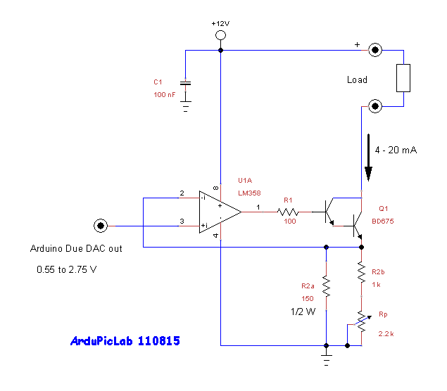
This has facilitated the design of an electronic circuit in order to obtain at the output a current range of 4 to 20 mA. The following diagram shows this simple circuit. It uses a single-rail LM358 operational amplifier and an NPN darlington transistor and a few other components.
The operational amplifier U1 and the transistor Q1 realize a tracking system, so that the voltage on emitter resistor R2 is equal to the input voltage.  Keeping constant the voltage on a resistor, by the Ohm's law, means that even the current is constant. In this way, the transistor emitter current Ie, flowing in R2, is dependent on the input voltage, therefore the circuit behaves as a current generator controlled by the input voltage.
From Kirchhoff's Current Law the collector current is: Ic = Ie – Ib, where Ib is the base current of transistor: Ib = Ic /hfe and hfe is the common-emitter current gain. Using a transistor with a hfe> 100 or greater, we can neglect the base current of the transistor and assert that also the collector current remains constant and proportional to the input voltage. A darlington transistor has an even greater current gain, so that we can assume that Ic = Ie.
The trimmer pot is used to adjust the maximum output current (20 mA) at the maximum number (4095) of the DAC or the maximum output voltage. This value, in the typical case of 3.3*5/6 is equal to 2.75 V, for which:
R2 = 2.75V /20mA = 137.5 Ω
In practice there may be slightly different values, therefore, it's better to use a potentiometer to precisely calibrate the current.
Powering the circuit with 5 V, supplied by of Arduino, the load can’t have higher voltages of 1 volt. Indeed, at 20 mA the voltage on R2 will be equal to about 2.75 V, which must be added to the Vce of the transistor which must not saturate. During the tests I used a digital ammeter that require a maximum of 0.2V on its terminals. For these reasons it is better to use higher supply voltages as 12 V or, better, 24 V. By varying the supply voltage does not involve variations of the circuit, but only an increase of dissipation on the transistor. In these cases a darlington medium power transistor is a good choice, as a TIP110, BD675, or similar.
 Don’t use operational amplifier as LM741, LM1458, TL081 and other that are not suitable for single-supply.
The photo below show the circuit, built on a bread board, during the test. For the interface with my Arduino Due system, I used a DB25 connector, mounted under the card.
To test the circuit, I wrote a simple program that sends to the DAC0  of Arduino Due, values of N according to the table: {0,512,1024,2048,3072,3584,4095}. They are generated in succession, each time I press the a button connected to pin 32. In the picture below you can see the circuit connected to my system, based on an Arduino Due and a LCD display. 
For the calibration measurements I used both a digital DMM, as shown in the photo, and a more accurate high resolution voltmeter on a precision 200.0 Ohm resistor, acting as load.
The results of these measurements were very good, as is also clear from the trend curve shown in the following figure and from R2, almost equal to one.
References
1)      “Atmel ARM Cortex-M3 Product Family (SAM3)”, Atmel application note 42187A−SAM−10/2013


Thursday, August 13, 2015

A very simple way to power Arduino

A simple and inexpensive solution is to use a 'mobile power bank', which is now widely available at low cost (from 5 €). The capacity of these systems is very high, almost always greater than 2000mAh, although some Chinese manufacturers print values ​​little true, as is the case for the batteries.
It is used to give energy to our smartphone or tablet, in cases in which our cellular battery is discharged or we can’t use the electricity grid. These devices incorporate, in a small volume, one or more rechargeable polymer battery, a charger (5V to 4.2V) and a step-up switching power supply to generate the 5V output from 3.6 V battery.
Normally it has two USB connectors female: output type A to power the phone or tablet and a micro USB for charging the internal battery, it connects to a normal power supply 5-5,5V 1 or 2 A, which is now a standard for the last generation mobile phones o tablets.
Usually they are provided of one or more cables to adapt to phones and tablet, typically with the micro USB or with standard iPhone connector. With the cable terminated with USB Micro, we can supply different cards, including Arduino Due, Yun, Nano and Teensy.
To power Arduino Uno we need a common USB cable A / B USB, like that used for printers.
This type of power supply is particularly suitable for portable and very compact systems, and it has an operating time of several hours. I use these devices for some years.

The photo below shows an example of an application with Arduino Yun.
With the experience of a few years of use of the power banks, may I suggest that you preferably use those that have a power switch. They cost more but do not have an internal consumption that significantly reduces battery life. In some cases I measured a battery discharge current of about 2 mA without any external load.

Monday, July 27, 2015

How to modify analog output range of Arduino Due

Arduino Due does not have an analog output voltage from 0 V to Vref, but from 1/6 to 5/6 of the reference voltage, that is, 0.55 V and 2.75V with Vref = 3.3 V. This is also confirmed by the Atmel (see bibliography).
The output voltage range of the DAC is only 2.75-0.55  = 2.2 V, with a resolution of 2.2/4095 = 0.5372 mV.
A simple differential amplifier, realized with an op amp, is used to remove the 0.55 V offset and to amplify the output signal in order to reach the desired value. The following figure shows the scheme of this circuit:

To generate the voltage Vp = 0.55 V, that is, the minimum value of the DAC, is used the divider formed by R3, R4 and Rp. The trimmer pot Rp is used to adjust Vp in order to have an output value close to 0 V in correspondence with the number 0 sent to the DAC. With a single power supply you can never get exactly 0V but you approach some mV, about 8 in my prototype.
The differential amplifier has the following gain:
G = Vo/(Vi-Vp) = R2 / R1
Just change the gain, for a different output voltage, but less than 4 V,.
With a gain G = 3.3 /2.2 = 1.5, the output of this circuit has  the desired range from 0 to 3.3V.

It is recommended to use resistors with a tolerance of 1% or less, particularly for the four resistors of the amplifier. Don’t use operational amplifier as LM741, LM1458, TL081 and other that are not suitable for single-supply.


References

1)      “Atmel ARM Cortex-M3 Product Family (SAM3)”, Atmel application note 42187A−SAM−10/2013

Monday, July 13, 2015

Teensy rev.3.1 and KS0108 Graphic LCD library

Giovanni Carrera 13/07/2015

This very interesting library, is still incompatible with the last version of Teensy.  The causes are at least two: the data ports of the MK20DX256 processor on Teensy are 32 bit against the 8 of ATmega328 on Arduino Uno, the second is the mapping used by the add-on program Teensyduino for the Arduino Ide, in order to make the compatibility with Arduino ONE, that has not a complete 8 bit I/O port available. For this reason the KS0108 library divides the GLCD data bus of eight bits in two nibbles: PortB (0:3) and PortD(4:7). PortC(0:4) is used for the control pins. The following table, shows the Arduino pins used for GLCD interfacing.

Arduino to GLCD wiring table
Arduino
 pin
GLCD signal
ATmega328
signal
8
DB0
PB0
9
DB1
PB1
10
DB2
PB2
11
DB3
PB3
4
DB4
PD4
5
DB5
PD5
6
DB6
PD6
7
DB7
PD7
A0
CS1
PC0
A1
CS2
PC1
A2
R/W
PC2
A3
D/I
PC3
A4
E
PC4
The use of two nibbles also causes a greater transfer time.
The teensyduino tries to make compatible Teensy with the Arduino I /O pins, but the hardware is completely different, since there is no  8-bit wise port. For this reason the KS0108 library is not compatible with Teensy 3.1.
Before starting to modify this library, I tried to see how the pin are organized with respect to the CPU port. The following table shows the CPU bit name and the corresponding Teensy pin name, that try to follow the Arduino Uno names. But the port bits are very different.
CPU
Teensy
Other
signal
 name
function
DAC0
DAC/A14

PTA12
3
CAN TX
PTA13
4
CAN RX
PTB0
16 /A2
SCL0/Touch
PTB1
17 /A3
SDA0/Touch
PTB16
0
RX1/Touch
PTB17
1
TX1/Touch
PTB2
19 /A5
SCL0/Touch
PTB3
18 /A4
SDA0/Touch
PTC0
15 /A1
Touch/CS
PTC1
22 /A8
Touch/CS/PWM
PTC2
23 /A9
Touch/CS/PWM
PTC3
9
RX2/CS/PWM
PTC4
10
TX2/CS/PWM
PTC5
13 (Led)
SCK
PTC6
11
DOUT
PTC7
12
DIN
PTD0
2
CS
PTD1
14 /A0
SCK
PTD2
7
RX3/DOUT
PTD3
8
TX3/DIN
PTD4
6
CS/PWM
PTD5
20 /A6
CS/PWM
PTD6
21 /A7
RX1/CS/PWM
PTD7
5
TX1/PWM


In order to overcome this problematic, I observed that there were two complete 8 bit port available, so I used the PORTD for data bus of the GLCD display, and I modified the library. In addition to the increased CPU speed, now the transfer is done with a single instruction.
The following table shows the pin assignment that have decided for the wiring with the display.
CPU
Teensy
Used by GLCD
signal
 name
PTA13
4
GLCD – R/W
PTB1
17 /A3
GLCD – E
PTB2
19 /A5
GLCD – CS1
PTB3
18 /A4
GLCD – CS2
PTC2
23 /A9
GLCD – /RST
PTC3
9
GLCD – D/I
PTD0
2
GLCD – DB0
PTD1
14 /A0
GLCD – DB1
PTD2
7
GLCD – DB2
PTD3
8
GLCD – DB3
PTD4
6
GLCD – DB4
PTD5
20 /A6
GLCD – DB5
PTD6
21 /A7
GLCD – DB6
PTD7
5
GLCD – DB7
As you can see, the order of the pins (2,14,7,8,6,20,21,5) does not respect one of the bits of the CPU portD.
After some test on I/O portD with 8 LEDs connected to port, I noted that they don’t respond to the logic of my program but they comply with the scrambled order of the table.
After an internet research, I found a good solution reading the hints of immortalSpirit (1). So I modify the I/O initialization in the library in the file ks0108_Teensy.h and in the main program ks0108.cpp, where I changed almost completely the function WriteData.
The system run now the graphic test GLCDexample.pde, as we can see in the following figure.

I have designed and made a very flexible project; in addition to the graphic display (a Winstar WG12864A, with RGB backlit), I added a SD card module and a real time clock, mounting a slim 32.768kHz quartz. On the top we can see a battery power bank that supplies the system for hours. An acrylic front panel preserves the GLCD .. and also creates the bad reflection on the photo.
With few changes I also ran on my Teensy GLCD, the program arduino-oscillo.pde of Noriaki Mitsunaga (3), an interesting oscilloscope which uses the same library and display. In the following figure the photo taken during the test.
References
  1. “Tutorial on digital I/O, ATMega PIN/PORT/DDR D/B registers vs. ARM GPIO_PDIR / _PDOR” - immortalSpirit - Jan 2013.
  2. "K20 Sub-Family Reference Manual”- Freescale - Document Number: K20P64M72SF1RM, Rev. 1.1, Dec 2012.
  3. “Arduino Oscilloscope”, Noriaki Mitsunaga, http://n.mtng.org/ele/arduino/oscillo.html